
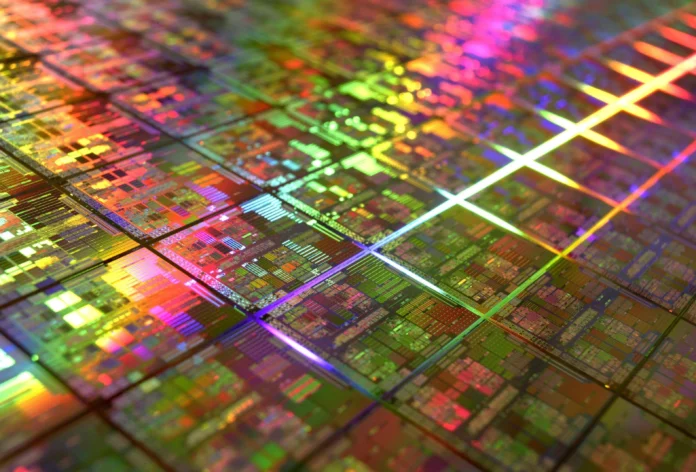
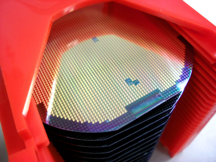
Silicon wafers are a substrate for all types of electronic devices and are mainly used to make electronic circuits due to their better conductivity and cost factor. They could get categorized as thin slices of pure silicon in crystallized form. This material is vital for manufacturing all semiconductors in almost every electronic device.
Patterned Silicon Wafers have the same caliber and purity as standard wafers. In addition to that, they pose better stability than unpatterned ones. The built-in patterns that get etched in silicon wafers enhance micro-electromechanical Systems (MEMS) and radio frequency (RF) processing as they get produced as per customers’ specialized requirements depending upon their device specifications.
Patterned Silicon Wafers Applications
Patterned silicon wafers get used in industries related to science, nanotechnology, electronics, and various other industries. The electronic components made with it work together to perform any given task as they are more stable. They get used in multiple gadgets worldwide. Few of their applications are in
Semiconductor Manufacturing
They are used in producing semiconductors of various forms and shapes that act as a building block in a wide range of electronic devices. It also gets included in circuited chips, diodes, and transistors.
These semiconductors get fabricated using these wafers, which provide compact concision and better cost-effectiveness. Since they can easily handle a different range of voltage produced by electricity, they also get used in all types of powered devices, optical sensors, and laser technology products.
Electronic And Computing Industry
Patterned silicon wafers get used extensively in the electronics and computing industry. They helped in boosting the present digital era. From manufacturing all types of microchips, ram chips, and any other electronic component with integrated circuits, wafers get used in one way or another to give an error-free enhanced performance.
Apart from the computing industry, they are commonly used in manufacturing devices used in home appliances, electronic systems, circuits in the automobile industry, smartphones, drone technology, and various other end products.
As new fabrication and automation technologies advance daily, these wafers get used in all electronic circuit-connected devices, making them more effective.
Optics Industry
These patterned wafers get used in the optics industry for the photonics that fabricates optical elements like optical fiber waveguides, filters for enhancing images, and others.
The pattern etched in the silicon wafer manipulates the transmission of light, enabling the creation of circuits relevant to the optic industry and other devices used.
All integrated image sensors used mainly in digital cameras have this wafer integrated into their semiconductors. Since these materials are economical, with fewer defects, they get used in reflective optics and infrared devices.
Manufacturing Solar Cells
Solar cells need these patterned silicon wafers, as it increases the efficiency to absorb more sunlight, increasing the cost-effectiveness of these cells.
The components used for manufacturing solar cells include monocrystalline and amorphous silicon, which requires a patterned wafer for better efficiency.
Aviation Industry
Due to their enhanced qualities and value, they are used in the aviation and aerospace industries. Mainly used as cover and permanent material in aviation, as it enhances the shielding and insulates the tools and different types of equipment that are delicate to heat and cold generated at extreme temperatures.
Since they can withstand high temperatures, these wafers are used widely in this industry. As rockets and aircraft equipment get frequently used, they undergo a lot of wear and tear. The manufacturers use silicon wafers to maintain or repair them.
Patterned Silicon Wafers Manufacturing
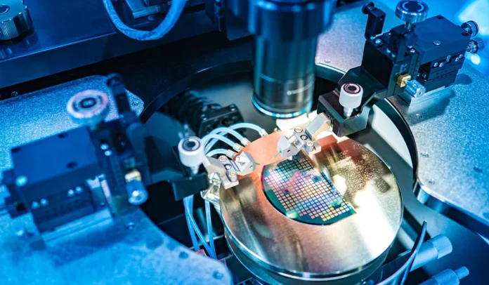
Manufacturing of wafers with built-in patterns, a mask oxide is grown that protects the surface of the wafer while patterning.
The sand that gets used to produce wafers should be pure silicon, and because of this, not all beach sand can get used. Mainly the sand from the beaches of Australia is shipped for silicon wafers manufacturing and then patterned as per the customer’s specifications. The process of manufacturing these patterned wafers includes,
Molten Silicon Preparation
When preparing the molten silicon, the sand gets heated up to thousand six hundred degrees celsius in a crucible. Once the sand melts, this molten sand becomes the starting point of silicon that will become the wafer.
Silicon Ingot Gets Made
The silicon in crystal form gets set down in the molten sand. After placing, this crystal is rotated and slowly pulled out. This technique is known as the Czochralski method.
This technique produces a cylinder-shaped silicon that is called an ingot.
Epitaxial Silicon
The epitaxial silicon growth gets done, providing a crystal clear surface for overdue processing.
This method uses chemicals to grow a silicon layer on the wafer. It increases the quality of the wafer layer. Processing gets done on this epitaxial layer.
As per the temperature fluctuations, the diameter of the ingot gets determined. It determines the rate at which the silicon ingot gets withdrawn.
When the ingot reaches the specified length, it gets removed and grounded to have an equal external diameter and surface.
Wafers Getting Prepared
After the ingot gets grounded into the required diameter for the wafers, it is sliced with a diamond saw to get thin wafers. They later get polished to remove defects and get the right thickness per the customer’s specification.
Photolithography Process
In this process, the wafer gets coated evenly with a thick light-sensitive liquid called photoresist. As the wafer is spinning, this coating gets applied to it.
Specific sections of the wafer get selected to align a mask between the ultraviolet light source and the wafer. The light source passes and exposes the photoresist wherever there is a transparent layer on the wafer, creating a pattern layer.
Direct Wafer Stepping Method
In this process, the mask layer is away from the wafer. The image gets put on the wafer through a series of optics. The mask can get slightly larger than the required pattern, but with the help of optical and mechanical frame-ups, a good portion could get exposed to a photoresist for better results.
The photoresists become impermeable to carving as it hardens when exposed to ultraviolet light. It helps remove the unexposed photoresist portion and thus leaving only the relevant required part on the patterned exposed wafer.
Wafer Surface Etching
Etching the Wafer Surface is done to remove any unwanted material from the wafer. These wafers get placed in a cage that rotates in a chemical etching solution.
It removes the damage that got created due to slicing and lapping. Usually, acid gets used in the etching solutions, but sometimes alkaline-based solutions are also used depending upon the requirement.
Polishing And Cleaning
The wafer gets polished by setting it onto a terracotta plate that gets pressed against the revolving plate covered in a polishing cloth.
Wafers are then cleaned with chemicals and ultra-pure water, giving them a mirror-like finish.
Conclusion
Patterned silicon wafers get used in all technologies that a human uses almost every day of life. It helps in the advancement of any given technology.
Due to its increased efficiency and functionality with customized designs, no other option element comes close to having better mechanical properties and cost-effectiveness. This product is going to rule the world for many centuries.


